EXPERIMENT No. 1
Identifying, Testing and Troubleshooting Semiconductor Components
Identifying, Testing and Combining Resistors
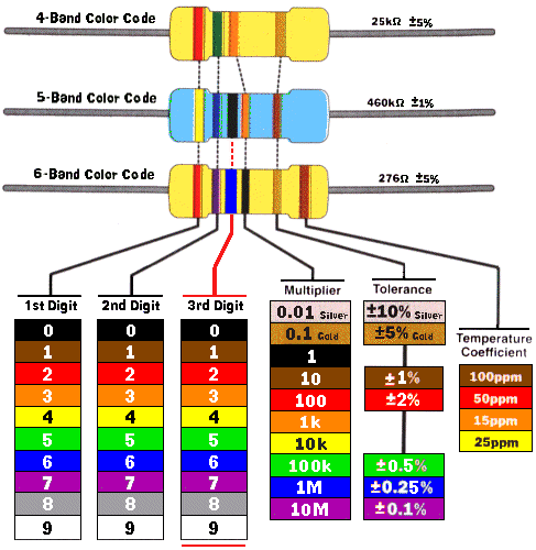
- First two or three bands may be the numbers to write down
- Next band is the multiplier (how many zeros to add to the number)
- Gold multiplier makes one decimal place smaller, Silver makes two decimal places smaller
- Last band to right may be tolerance values
- Notice the examples on the right
- Brown, red, red = 1, 2, 100, 5% = 1200Ω 5%, or 1.2KΩ,1K2
Obtain 6 resistors of different values. You are then going to determine their value two ways:
· Use the colour code to calculate the value of the resistor.
· Include the maximum and minimum tolerance value of each resistor
· Then measure the resistor value with a multimeter.
Record the values in the chart below:
| Value (colour codes ) | Value (multimeter) |
| | |
| | |
| | |
| 5320Ω—5880Ω(5.32kΩ—5.88kΩ ) | |
| | |
| | |
Choose two resistors and record their individual ohm resistance value measured with a multi-meter:
Resistor 1 ____99____ Ω Resistor 2 ___268.8___ Ω
Put these two resistors together in series (end to end, one right after another) calculate and then measure their combined value. Show workings:
Calculated value 1 and 2 in series: ____366.8____ Ω
Measured value 1 and 2 in series: ____366.8____ Ω
Put these two resistors together in parallel (connect both ends when they are side-by-side). Calculate and then measure their combined value. Show workings:
Calculated value 1 and 2 in parallel: ___72.5____ Ω
Measured value 1 and 2 in parallel: ____72.5____ Ω
What principles of electricity have you demonstrated with this? Explain:
EXPERIMENT No. 2
DIODES

A diode has the characteristics of:
· An insulator when current tries to flow in one direction.
· A conductor when current flows in the other direction.
Components: 1 x diode, 1 x LED
Exercise: Using a multimeter, identify the anode and cathode of the diode and the LED.
| | Voltage drop in forward Biased Direction. | Voltage drop in reverse biased direction |
| LED | | |
| Diode | | |
Explain how you could identify the cathode without a multimeter
Theres a edge cut out on the LED to represent cathode.
Table 1: Data sheet of 1N4007 is as follows
| Absolute Maximum Ratings, TA = 25OC | |||
| Symbol | Parameter | Value | Units |
| IO | Average rectified current @ TA = 75oC | 1.0 | A |
| PD | Total device dissipation Derate above 25oC | 2.5 20 | W mW/OC |
| | Thermal resistance, Junction to Ambient | 50 | OC/W |
| | | -55 to + 175 | OC |
| | Operating | -55 to + 150 | OC |
| VRRM (PIV) | Peak repetitive reverse voltage | 1000 | V |
Components: 1 x resistor, 1 x diode. 1 x LED
Exercise: For Vs=5V, R= 1KΩ, D= 1N4007 build the following circuit on a breadboard.

Fig 5
Calculate first the value of current flowing through the diode, now measure and check your answer?
Show your working
Calculated Measured
I=V/R 0.0043A
I=5-0.7/1000Ω=0.0043A
Is the reading as you expected; explain why or why not?
It's my expect reading, cause diode takes away 0.7V, and resistance is 1000Ω, so I=0.0043A,.
Calculate the voltage drop across the diode, now measure and check your answer?
Calculated Measured
Vd=IxR 0.66Vd
Vd=5-0.0043x1000=0.7Vd
Using the data sheet given in Table 1 above,
What is the maximum value of the current that can flow through the given diode?
In table 1, the maximum value of the current that can flow through the diode is 1A.
For R = 1KΩ. What is the maximum value of Vs so that the diode operates in a safe region?
V=IR=1000×1=1000Ω
Replace the diode by an LED & calculate the current, then measure and check your answer?
Calculated Measured
I=V/R 0.003A
I=5-1.95/1000=0.003A
What do you observe? Explain briefly.
LED and resistor are connected in series, and LED takes away 1.95V, so calculated value is 3.05 ma.
EXPERIMENT No. 3
Components: 2 x resistors, 1 x 5V1 400mW Zener diode (ZD).
Exercise: Obtain a breadboard, suitable components from your tutor and build the following circuit.

Fig 6
For R= 100Ω and RL= 100Ω, Vs= 12 V.
What is the value of Vz?
Vz=4.96V
Vary Vs from 10V to 15 V
What is the value of Vz
The value at Vz Varied from 10V to 15V 4.85V, 5.01, 5.05, 5.10
Explain what is happening here
This circuit is restricting flow so its regulating the volts at around 4.6V.
This circuit could be used for regulating voltage in a circuit.
Reverse the polarity of the zener diode.
What is the value of Vz? Make a short comment why you had that reading.
After Reversing the polarity of the zener diode it went from 4.68v on 10v to 840mV because when the diode is reversed it stops the flow of power through it but it doesn't completely stop all power flowing through just a small amount.
EXPERIMENT No. 4
Components: 1 x resistors, 1 x 5V1 400mW Zener diode, 1X Diode1N4007 .
Exercise: Obtain a breadboard, suitable components from your tutor and build the following circuit.
Vs=10 & 15v, R=1K ohms

Fig 7
10 Volts 15 Volts
Volt drop V1: 4.62Vd 4.77Vd
Volt drop V2: 0.67Vd 0.69Vd
Volt drop V3: 5.29Vd 5.47Vd
Volt drop V4: 5.24Vd 9.68Vd
Calculated current A: I=10V/1000Ω=0.01A I=15V/1000Ω=0.015A
Describe what is happening and why you are getting these readings:
The current flows through the resistor and the diodes and the power gets used up as it goes through the circuit so all the answers i got where correct because they all added up to the supply voltage.
EXPERIMENT No. 5
The Capacitor

The capacitor stores electric charge.
A capacitor consists of two metal plates very close together, separated by an insulator. When connected to a battery or power source electrons flow into the negative plates and charge up the capacitor. The charge remains there when the battery is removed. The charge stored depends on the “size” or capacitance of the capacitor, which is measured on Farads (F).
Types of capacitor:
| Non-electrolytic capacitor | |
 | · Fairly small capacitance - normally about10pF to 1mF · No polarity requirements - they can be inserted either way into a circuit. · Can take a fairly high voltage. |
| Variable capacitor | |
 | · Adjustable capacitor by turning a knob - similar to variable resistors. · The maximum capacitance available is about 200pF. · Used in radios. |
| Electrolytic capacitor | |
 | · Large capacitances - 1mF to 50000mF · Warning: These must be corrected the right way round (polarity) or they can explode - the white terminal on the diagram above signifies positive. · Black stripe with “-“ shows which terminal is the negative (usually the short one) · Low voltage rating – from 25 ~ 100V DC · They have a significant leakage current - this means that they will lose the charge stored over time. |
| Tantalum capacitor | |
 | · These have the same properties as the Electrolytic capacitor, but they are physically smaller & have lower leakage. As a result, though, they are more expensive. |
Identifying Capacitor “Size”
If the Farad “size” is not printed on the capacitor, you may find an EIA code listed. Use the table below to figure out the capacitance
| μF | nF | pF | EIA Code |
| 0.00001* | 0.01 | 10 | 100 |
| 0.0001* | 0.1 | 100 | 101 |
| 0.001 | 1.0 (1n0) | 1,000 | 102 |
| 0.01 | 10 | 10,000* | 103 |
| 0.1 | 100 | 100,000* | 104 |
| 1.0 | 1000* | 1,000,00* | 105 |
| 10.0 | 10,000* | 10,000,00* | 106 |
* Values with asterisk are not usually expressed in this form
RC Time Delay or “Charging Time”
Capacitors take time to charge. It doesn’t happen instantly. The charge time is dependent on the resistor in the circuit and the size of the capacitor. And it is expressed in the equation: R x C x 5 = T. This is the time it takes to charge up to the applied voltage.
For example, 1,000,000 Ω x 0.000001 F x 5 = 5 seconds to charge to applied voltage. This can also be expressed as 1 MΩ x 1 μF x 5 = 5 seconds.
Capacitors are often used for timing when events take place. And often the voltage only has to get up to about 2/3 the applied voltage, and this happens at about 1/5 the time of their charging. So this is why the 5 is built into the equation. The concept of “time constants” is used here, where whatever the time it takes for a capacitor to build up to the full charge, it takes about 1/5 of that time to build up close to 2/3 of the charge. So you can divide the charge time into 5 segments, and the first time segment is often the time you are interested in.
Practice watching the capacitors charge up in the exercise below.

Fig 8-Capacitor Charging Circuit
Components: 1 x resistor, 1 x capacitor. 1 x pushbutton N/O switch.
Exercise: First, calculate how much time it would take to charge up the capacitor. Then, connect the circuit as shown above. Measure the time taken by the capacitor to reach the applied voltage on an oscilloscope. Fill in the chart below. Also draw the observed waveforms in the graphs below, filling the details on each one.
Note: you will need to adjust the time base to enable you to observe the pattern.
| Circuit number | Capacitance (uF) | Resistance (KΩ) | Calculated Time (ms) | Observed Time (ms) |
| 1 | 100 | 1 | | |
| 2 | 100 | 0.1 | | |
| 3 | 100 | 0.47 | | |
| 4 | 330 | 1 | | |
Label the axis of each graph:
Circuit 1:

Capacitance 100uf Resistance 1000Ω
Circuit 2:

Capacitance 100uf Resistance 100Ω
Circuit 3:

Capacitance 100uf Resistance 470Ω
Circuit 4:

Capacitance 330uf Resistance 1000Ω
How does changes in the resistor affect the charging time?
How does changes in the capacitor affect the charging time?
The higher the uf capacitor the longer it takes to charge
EXPERIMENT No. 6
Meter check of a transistor
Bipolar transistors are constructed of a three-layer semiconductor “sandwich,” either PNP or
NPN. As such, transistors register as two diodes connected back-to-back when tested with a
multimeter’s “diode check” function as illustrated in Figure 9.1. Low voltage readings on the base with the black negative (-) leads correspond to an N-type base in a PNP transistor. On the symbol, the N-type material corresponds to the “non-pointing” end of the base-emitter junction, the base. The P-type emitter corresponds to “pointing” end of the base emitter junction the emitter.
9.1: PNP transistor meter check: (a) forward B-E, B-C, voltage is low; (b) reverse
B-E, B-C, voltage is OL.
BIPOLAR JUNCTION TRANSISTORS
Here I’m assuming the use of a multimeter has a diode test function to check the PN junctions.
If your meter has a designated “diode check” function, and the meter will display the actual forward voltage of the PN junction and not just whether or not it conducts current.
Meter readings will be exactly opposite, of course, for an NPN transistor, with both PN
junctions facing the other way.
Low voltage readings with the red (+) lead on the base is the “opposite” condition for the NPN transistor. If a multimeter with a “diode check” function is used in this test, it will be found that
the emitter-base junction possesses a slightly HIGHER forward voltage drop than the collector
base junction. This forward voltage difference is due to the disparity in doping concentration
between the emitter and collector regions of the transistor; the emitter is a much more heavily
doped piece of semiconductor material than the collector, causing its junction with the base to
produce a higher forward voltage drop.
Knowing this, it becomes possible to determine which terminal is which on an unmarked transistor.
This is important because transistor packaging, unfortunately, is not standardised. All
bipolar transistors have three terminals, of course, but the positions of the three terminals on the actual physical package are not arranged in any universal, standardised order.
Suppose a technician finds a bipolar transistor and proceeds to measure voltage drop with a
multimeter set in the “diode check” mode. Measuring between pairs of terminals and recording the
values displayed by the meter, the technician obtains the data in Figure 9.2.
Figure 9.2: Unknown bipolar transistor. Which terminals are emitter, base, and collector?
-meter readings between terminals.
The only combinations of test points giving conducting meter readings are terminals 1 and 3
(red test lead on 1 and black test lead on 3), and terminals 2 and 3 (red test lead on 2 and black test lead on 3). These two readings must indicate forward biasing of the emitter-to-base junction
(0.655 volts) and the collector-to-base junction (0.621 volts).
Now we look for the one terminal common to both sets of conductive readings. It must be the
base connection of the transistor, because the base is the only layer of the three-layer device
common to both sets of PN junctions (emitter-base and collector-base). In this example, that
terminal is number 3, being common to both the 1-3 and the 2-3 test point combinations.
METER CHECK OF A TRANSISTOR
Those sets of meter readings, the black (-) meter test lead was touching terminal 3, which tells us
that the base of this transistor is made of N-type semiconductor material (black = negative).
Thus, the transistor is a PNP with base on terminal 3, emitter on terminal 1 and collector on terminal 2 as described in Figure 9.3.
 E and C reverse: 1(+) and 2(-): “OL”
- E and C reverse: 1(-) and 2(+): “OL”
- E and B forward: 1(+) and 3(-): 0.655 V
- E and B forward: 1(-) and 3(+): “OL”
- C and B forward: 2(+) and 3(-): 0.621 V
- C and B forward: 2(-) and 3(+): “OL”
Figure 9.3: BJT terminals identified by meter.
Please note that the base terminal in this example is not the middle lead of the transistor, as one
might expect from the three-layer “sandwich” model of a bipolar transistor. This is quite often
the case, and tends to confuse new students of electronics. The only way to be sure which lead
is which is by a meter check, or by referencing the manufacturer’s “data sheet” documentation
on that particular part number of transistor.
Knowing that a bipolar transistor behaves as two back-to-back diodes when tested with a
Diode test function is helpful for identifying an unknown transistor purely by meter readings.
It is also helpful for a quick functional check of the transistor. If the technician were to measure
Using the Diode test function in any more than two or any less than two of the six test lead combinations, he or she would immediately know that the transistor was defective (or else that it wasn’t a bipolar transistor but rather something else – a distinct possibility if no part numbers can be referenced for sure identification!). However, the “two diode” model of the transistor fails to
explain how or why it acts as an amplifying device.
Transistor Symbol and semiconductor construction shown below.
|
PNP NPN
Fig 10
Identify the legs of your transistor with a multimeter. For identifying and testing purposes, refer to the representation shown above.
| Diode test (V) meter readings | ||||||
| Transistor number | VBE | VEB | VBC | VCB | VCE | VEC |
| NPN | | | | | | |
| PNP | | | | | | |
EXPERIMENT No. 7
Transistor as a switch
Components: 1 x Small Signal NPN transistor, 2 resistors.
Exercise: Connect the circuit as shown in Fig 12 and switch on the power supply.

Fig 12
Connect the multimeter between base and emitter.
Note the voltage reading and explain what this reading is indicating.
Connect the multimeter between base and emitter, the voltage reading is 0.797V, it indicates the voltage drop cross B and E is 0.797V, when it starts to work.
Connect the multimeter between collector and emitter.
Note the voltage reading and explain what this reading is indicating.
Connect the multimeter between collector and emitter, the voltage is 54.5mV, it indicates when voltage drop cross B and E is 0.797V, when it starts to work, the voltage drop cross C and E is 54.5mV.
In the plot given below what are the regions indicated by the arrows A & B?

|
Fig 13
How does a transistor work in these regions? Explain in detail:
At Vce 5 the Ib = approx 0.2 mA Ic 5mA the transistor starts to operate and as the Vce volts decrease
the Ic mA and Ib mA increase the transistor becomes fully operational at approx Vce 1v, Ic 30mA, Ib 1mA
What is the power dissipated by the transistor at Vce of 3 volts?
P=IxV=14mA x 3v = 42 mA
What is the Beta of this transistor at Vce 2,3 & 4 volts?
2 Vce = Ic/Ib=20 Ic mA ÷ 0.8 Ib mA = 25 Beta
3 Vce = Ic/Ib=14 Ic mA ÷ 0.5 Ib mA = 28 Beta
4 Vce = Ic/Ib=5 Ic mA ÷ 0.2 Ib mA = 25 beta
EXPERIMENT No. 8
Summary: Vary the base resistor and measure changes in voltage and current for Vce, Vbe, Ic, and Ib. Then plot a load line.
Set up the following circuit on a bread board. Use a 470R for Rc and a BC547 NPN transistor.

Pick five resistors between 2K2 and 1M for Rb. You want a range of resistors that allow you to see Vce when the transistor is the saturated switch region and when it is in the active amplifier region. I used 47K, 220K, 270K, 330K and 1M, but this can vary depending on your transistor. Some may need to use 2K2. Put one resistor in place, and measure and record voltage drop across Vce and Vbe. Also measure and record the current for Ic and Ib. Then change the Rb resistor and do all the measurements and record the new readings. Do this for each of the resistor values above.
Record here:
Rb 46.7K Vbe: 0.72V Vce: 0.119mV Ib:52.51uA Ic:6.5mA
Rb 220K Vbe: 0.684V Vce:1.783V Ib:11.4uA Ic: 3.06mA
Rb 265K Vbe: 0.678V Vce: 2.02V Ib: 9.6uA Ic: 2.5mA
Rb 330K Vbe: 0.678V Vce: 2.25V Ib: 7.7uA Ic: 2.07mA
Rb 988K Vbe: 0.642V Vce: 2.94V Ib: 2.6uA Ic: 0.7mA
Your voltage drop measurements across Vce should vary from below 0.3 v (showing the transistor is in the saturated switch region) to above 2.0 v (showing the transistor is in the active amplifier region) If this is not the case, you may have to try a smaller or bigger resistor at Rb. Talk to your teacher to get a different size resistor, and redo your measurements.
Discuss what happened for Vce during this experiment. What change took place, and what caused the change?
With the same supply voltage 5V, as Rb gets larger, Vce gets larger and this because the transistor is getting thurther away from being in the saturated region and the transistor is not hard switching..
Discuss what happened for Vbe during this experiment. What change took place if any, and what caused the change?
With the same supply voltage 5V, as Rb gets higher, Vbe gets lower.
Discuss what happened for Ib during this experiment. What change took place, and what caused the change?
Discuss what happened for Ic during this experiment. What change took place, and what caused the change?
On the ic side the same thing is happerning as the ib side of the circuit and this is because the resistance at rb is controling how much the transistor is opening, limitering how much current can go through the transistor.
Plot the points for Ic and Vce on the graph below to create a load line. Plan the values for so you use up the graph space. Use Ic as your vertical value, and Vce as your horizontal value.
Using Vbe on the Vce scale, plot the values of Ib so the finished graph looks similar to fig 13
Calculate the Beta (Hfe) of this transitor using the above graph.
When Rb=46.7K, Beta=6.5/52.51X1000=123.8;When Rb=220K, Beta=3.06/11.4X1000=268.4
When Rb=265K, Beta=2.5/9.6X1000=260;When Rb=330K, Beta=2.07/7.7X1000=268.8
When Rb=988K, Beta= 0.7/2.6X1000=269.2
Explain what the load line graph is telling you. Discuss the regions of the graph where the transistor is Saturated, Cut-off, or in the Active area.
Ib and Ic changed because as different size resistors were used they restricted differently allowing more or less current to flow through the circuit.Region A is the time when transistor is saturated, region B is the time when transistor is cut off, region C is the time when transistor is active.
Leo, its very hard to read your blog. For your next blog could you please change the colour? Also theres too much of the Labwork sheet that you copied on there, you must put it in your own words & reference it. You barely passed this blog so make your next one better.
回复删除