Using the dual trace feature on the oscilloscope capture the full pattern of the H-CAN and L-CAN. Identify which wire is the H-CAN and which is for the L-CAN.
H-CAN: Blue L-CAN:Yellow They both connected to the positone
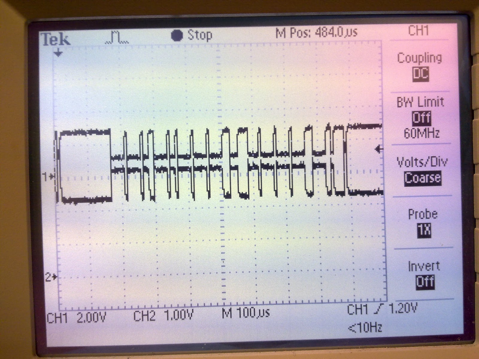
On your capture also identify were the data pattern starts and finishes.

The top one patterns is the low can they start off normal and they drop down, the botton one is high can patterns they start off normal and then it jumps up and this test was done without wipers or light on .
For each of the following inputs capture the pattern and identify were it changes in relation to the original pattern:
Right indicator
Rear wiper

Reverse lights

Fuel pump

Using the wiring diagram and CAN board Identify the input /output pins, wire colours, Relay or transistor for the right hand indicator and rear wiper:
I choose right hand indicator that starts off with pin 7, it goes to resistor 5 after that it goes to chip 6 -vp18f258/ra4/tocki then it comes out through can-high and can- low straight though channel 1 and then it foes out through con 1 and 2 though 4 and 5 then it goes to the can ship into 7 and 6 goes out through 4 all the way straight to 12 /rxcan/n which is the iC chip then it goes through 5 pass through resistor 32. After that it into the optocaupler the it goes out passes through pull down resistor goes to the transistor then it travels to the connector output 5.
Using the wiring diagram identify both voltage regulators that resemble the one that you built in TTEC4824. Note all the input pins and were the outputs are connected to.
U1 7805: Input from power supply P1 & P2
Output is 5V, it goes to P1 (MCLR/VPP) & P20 (VE) on chip VP18F258 P3 (VCC) goes to chip IC4, P16 goes to chip IC3
U2 7805: Input from power supply P1 & P2
Output is 5V, it goes to P14 (VDD)
Using the wiring diagram follow one circuit though from the input to the output. Note all the inputs / IC / relays / transistors and describe how the circuit operates
Spare: P10 goes to R7 (14500) then input to P26 on chip VP18F258. Output to P23 & P24, P23 &P24 both goes to chip IC4 and output to P7 & P6, P7 goes to P1, P6 goes to CAN connector P2, P7 & P6 also goes through standared terminal.
Output: P8 goes to RL5b switch when the switch cloesd the RL5a will goes to the transistor U15 then goes to R36 (1K) after input to P1 on chip DIL then P11 comes out to P12 & 13, they input to P1 &P4 on chip IC5 and comes out to P7 & P6 then goes to P4 & P5
没有评论:
发表评论